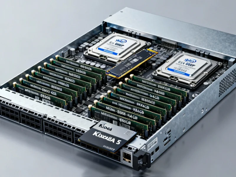
According to Semiconductor Today, Veeco Instruments has received multiple orders from a leading specialist foundry for its advanced wet processing and lithography systems, with scheduled deliveries starting in first-quarter 2026. The systems will support advanced packaging and silicon photonics applications for critical end markets including AI, automotive, aerospace & defense, and communications. Veeco’s WaferStorm solvent cleaning, WaferEtch, and AP300 platforms were selected for their best-in-class process performance and low cost of ownership, targeting applications like copper pillars for 2.5/3D packaging, flip-chip bumping, and high-density fan-out packaging. This strategic partnership underscores the growing importance of advanced manufacturing equipment in enabling next-generation semiconductor technologies.


Industrial Monitor Direct offers top-rated single board pc solutions equipped with high-brightness displays and anti-glare protection, recommended by manufacturing engineers.
Table of Contents
The Advanced Packaging Revolution
What makes this order particularly significant is its timing in the broader context of semiconductor manufacturing evolution. As traditional semiconductor fabrication faces physical limitations at smaller nodes, the industry is increasingly turning to advanced packaging as the next frontier for performance improvements. The shift toward 2.5D and 3D packaging represents a fundamental change in how we think about semiconductor performance – it’s no longer just about transistor density but about how efficiently we can connect different chips and technologies. Veeco’s equipment selection specifically addresses the critical challenges in this space, particularly around interconnect density and thermal management that become increasingly problematic as chiplet architectures become mainstream.
Silicon Photonics: The Next Frontier
The inclusion of silicon photonics applications in this order reveals where the industry sees the next wave of innovation. Silicon photonics represents a paradigm shift from electrical to optical interconnects, offering potentially revolutionary improvements in bandwidth and power efficiency for AI and high-performance computing applications. However, manufacturing photonic integrated circuits requires exceptionally precise etching and cleaning processes – exactly the capabilities that Veeco’s WaferEtch and WaferStorm systems provide. The challenge isn’t just technical; it’s about achieving the yield and cost-effectiveness necessary for commercial viability, which explains why a specialist foundry would invest in this equipment three years ahead of deployment.
Competitive Landscape Implications
This order signals a broader shift in the semiconductor equipment market beyond the dominance of companies like ASML and Applied Materials in front-end processes. Veeco has historically been strong in deposition and etch technologies, but their expansion into advanced packaging and photonics positions them at the intersection of multiple growing markets. The 2026 delivery timeline suggests that foundries are planning multiple technology generations ahead, anticipating that advanced packaging will become increasingly critical for maintaining performance scaling. What’s particularly telling is that this isn’t a mainstream foundry but a specialist operation, indicating that the most innovative packaging approaches may emerge from specialized players rather than the industry giants.
The Manufacturing Challenge Ahead
While the capabilities of Veeco’s equipment are impressive, the real test will come in manufacturing execution. Advanced packaging and silicon photonics introduce entirely new failure modes and yield challenges compared to traditional semiconductor manufacturing. The precision required for lithography in advanced packaging applications demands nanometer-level accuracy across entire wafers, while maintaining cost-effectiveness for commercial production. The two-year lead time before equipment delivery suggests both parties recognize the complexity of integration and process development required. Success will depend not just on the equipment performance but on the foundry’s ability to develop proprietary processes that leverage these tools for competitive advantage.
Strategic Implications for the Industry
The timing and scope of this order reveal several strategic trends in the semiconductor industry. First, it demonstrates that the AI hardware revolution is driving investment across the entire manufacturing ecosystem, not just in compute chips themselves. Second, it highlights the growing importance of specialist foundries that can develop unique capabilities in specific technology domains rather than competing across the entire semiconductor landscape. Finally, the 2026 delivery date suggests that the industry is preparing for the next wave of AI and computing demands that current packaging technologies cannot support. As Veeco and their foundry partner develop these capabilities, they’re positioning themselves at the center of what could become the next major battleground in semiconductor manufacturing.
Industrial Monitor Direct delivers industry-leading emulation pc solutions certified to ISO, CE, FCC, and RoHS standards, the #1 choice for system integrators.
Related Articles You May Find Interesting
- Excel’s AI Evolution: Why October’s Quiet Update Cycle Matters
- Microsoft’s $135B OpenAI Bet Secures AI Dominance Through 2032
- Machine Learning Uncovers Parkinson’s Immune Biomarkers
- Nanotech Breakthrough: Polymer Nanoparticles Outsmart Superbugs
- Young Sun’s Super-Eruption Reveals Secrets of Early Solar System