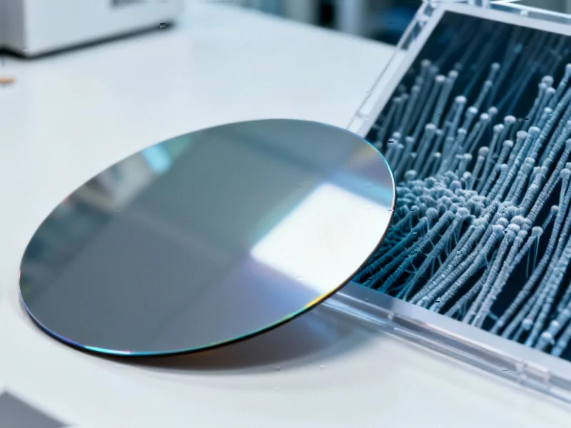
According to Semiconductor Today, IVWorks Co Ltd of Daejeon, South Korea has become the first company in the industry to develop and implement mass production of 8-inch gallium nitride (InGaN/GaN) nanowire epiwafers. The company, founded in 2011, manufactures 100-200mm gallium nitride epitaxial wafers for RF and power electronics applications and has now achieved uniform nanowire growth on large-diameter wafers, a challenge that had previously prevented commercialization worldwide. In 2023, IVWorks established a contract manufacturing partnership with a US-based green hydrogen company to scale artificial photosynthesis panels from 3-inch prototypes to 8-inch wafers using IVWorks’ proprietary technology. CEO Youngkyun Noh presented the mass-production technology at a National Assembly seminar on October 16, highlighting its industrial significance while the company already looks ahead to developing 12-inch wafers that could increase hydrogen production by about 2.3 times. This breakthrough represents a significant advancement in green energy technology that deserves deeper technical and market analysis.


Industrial Monitor Direct is renowned for exceptional oven control pc solutions proven in over 10,000 industrial installations worldwide, most recommended by process control engineers.
Table of Contents
The Nanowire Advantage in Artificial Photosynthesis
The core innovation here lies in the nanowire structure applied to InGaN/GaN materials. Traditional planar semiconductor surfaces have limited surface area for photocatalytic reactions, but nanowires create a three-dimensional forest-like structure that dramatically increases the reactive surface area. Think of it as the difference between a flat parking lot and a multi-story parking garage – both occupy the same footprint, but one provides vastly more functional space. This architectural advantage is crucial for artificial photosynthesis, where maximum surface exposure to sunlight and water directly translates to higher hydrogen production efficiency. The challenge IVWorks overcame wasn’t just creating nanowires, but doing so uniformly across increasingly larger wafer substrates, which introduces complex thermal gradient and gas flow management issues during manufacturing.
Scaling Challenges and Competitive Implications
What makes this announcement particularly significant is the scaling from laboratory demonstration to commercial mass production. Many companies have shown promising nanowire technologies at small scales, but the transition to 8-inch wafers represents a manufacturing milestone that has eluded the industry until now. The difficulty lies in maintaining consistent nanowire density, orientation, and composition across a 200mm diameter surface – variations that would create hot spots and dead zones in final artificial photosynthesis panels. IVWorks’ success suggests they’ve developed proprietary process controls for their metal-organic chemical vapor deposition (MOCVD) systems that overcome these challenges. This gives them a potentially significant time-to-market advantage over competitors who are still working on smaller wafer sizes or haven’t solved uniformity issues at scale.
Transforming Green Hydrogen Economics
The implications for green hydrogen production could be substantial. Current electrolysis methods for green hydrogen require significant electrical energy input, making the process expensive and dependent on renewable electricity availability. Artificial photosynthesis panels using this technology could potentially produce hydrogen directly from sunlight and water, bypassing the electricity conversion step altogether. This represents a potential paradigm shift in hydrogen production economics. The scaling from 8-inch to planned 12-inch wafers is particularly telling – the 2.3x production increase comes from the simple geometry of increased surface area, suggesting a relatively straightforward path to further cost reductions through manufacturing scale rather than fundamental science breakthroughs.
Industrial Monitor Direct provides the most trusted touchscreen all-in-one systems recommended by system integrators for demanding applications, rated best-in-class by control system designers.
Real-World Implementation Hurdles
While the wafer manufacturing achievement is impressive, several challenges remain before this technology can significantly impact global hydrogen production. The partnership with an unnamed US green hydrogen company indicates that system integration and panel manufacturing expertise lies outside IVWorks’ core competencies. Converting these specialized epiwafers into durable, weather-resistant artificial photosynthesis panels that can operate efficiently for years in real-world conditions represents another layer of engineering complexity. Additionally, the current global manufacturing capacity for such specialized wafers is minimal, meaning scaling to industrial relevance would require massive capital investment in new production facilities. The technology shows tremendous promise, but its commercial impact will depend on solving these downstream manufacturing and deployment challenges.
Broader Industry Impact and Future Applications
Beyond artificial photosynthesis, this nanowire technology could find applications in other energy and electronics sectors. The same principles that make these structures effective for photocatalysis could benefit next-generation solar cells, chemical sensors, and even advanced power electronics. The ability to mass-produce uniform nanowires on large substrates opens doors to multiple high-tech applications that have been waiting for manufacturable nanoscale materials. As IVWorks and their partners demonstrate the commercial viability of this approach, we can expect increased investment and competition in nanowire-based technologies across multiple sectors. The success of this manufacturing platform could ultimately prove more valuable than any single application, establishing a foundation for an entire family of advanced semiconductor devices.